If you haven't already seen from some of the other websites in the LaunchPad community, TI is gearing up to release more MSP430 devices that are compatible with the LaunchPad. Some of these will be 20-pin chips, and will make use of the entire board. You can see details of the new devices on TI's website.
In regards to the new devices, some will include more of the MSP430 peripherals, most notably a hardware UART for serial communication. The UART uses the same two pins that TI chose to use on the LaunchPad for the timer-based UART used in the demo program that comes with the G2231 chip. Unfortunately, it swaps the transmit and receive functions on these pins. TI is working on potentially re-designing the LaunchPad, and has asked for the community's views on how to approach this issue. If you haven't already, go to the post on the E2E Community site, review the proposals they've given, and vote for the solution you think is best!
29 December 2010
27 December 2010
Tutorial 12: Making Comparisons
As we've seen, microcontrollers have great usefulness in digital electronics. In the real world, and for scientific applications, however, digital is not always adequate. In this tutorial, we begin working with analog signals using a 1 bit analog to digital converter: the comparator.
Some MSP430 devices have a built-in comparator (called the Comparator_A+ module in the technical documentation, I'll refer to it as CA+ here), including the MSP430G2211 that comes with the LaunchPad kit. (See TI's website for other LaunchPad-compatible devices that include the CA+ module.) Up to this point, all of the tutorials could be used on both the G2211 and the G2231 chips in the LaunchPad kit by changing the #include header appropriately. For this tutorial, you will need to use the G2211.
Overview of the Comparator_A+ Module
The CA+ module is very flexible, allowing multiple GIO pins to be connected to its inputs and including a variety of useful internal voltage references. As you may recall, a comparator has two inputs, called inverting and non-inverting (often labeled V+ and V- respectively). The V+ input can be connected to three different pins for external signals, or any of three different internal reference signals. The V- input can be connected to seven different pins (two overlap with the V+ inputs) and any of the internal references. CA+ has an output that can be read in software, trigger the CA+ interrupt, and trigger a timer interrupt. All of these options give the CA+ module its flexibility and usefulness to us in developing instrumentation.
 |
| Simplified diagram of the Comparator_A+ module. Taken from the book MSP430 Microcontroller Basics |
The CA+ module is very flexible, allowing multiple GIO pins to be connected to its inputs and including a variety of useful internal voltage references. As you may recall, a comparator has two inputs, called inverting and non-inverting (often labeled V+ and V- respectively). The V+ input can be connected to three different pins for external signals, or any of three different internal reference signals. The V- input can be connected to seven different pins (two overlap with the V+ inputs) and any of the internal references. CA+ has an output that can be read in software, trigger the CA+ interrupt, and trigger a timer interrupt. All of these options give the CA+ module its flexibility and usefulness to us in developing instrumentation.

Take a look at the datasheet for the G2211, and find the page that shows the pinout diagram for the chip. The pins that can be connected to the CA+ inputs are labeled as CAx. Note that CA0-2 can be connected to V+, while CA1-7 can be connected to V-. Note also that in addition to providing the CA7 input, P1.7 can be configured to provide the output value CAOUT externally.
Configuring the Comparator_A+ module
The CA+ module has three different registers for its configuration: CACTL1, CACTL2, and CAPD. These registers are described on pages 19-10 to 19-13 of the x2xx Family Guide. We'll look at the basic pieces here.
CACTL1

- The CAREFx and CARSEL bits (4-5 and 6) control the internal references for the comparator. Bits 4 and 5 select the reference value, while bit 6 selects which input is connected to the reference. There are three references provided in the module. Two of them are a fractional value of the voltage powering the MSP430: 1/2 Vcc and 1/4 Vcc. If you are powered from the USB (3.6 V), these references are 1.8 V and 0.9 V respectively. (These are accurate to about 1%.) A third reference is provided by the forward voltage of a transistor. This voltage is typically 0.55 V, but is less accurate and susceptible to temperature changes.
- The CAIFG, CAIE, and CAIES bits (0-2) control the interrupt for the comparator. Bit 0 is the interrupt flag, which clears automatically when the interrupt is serviced. Bit 1 turns on the interrupt, and bit 2 selects whether an interrupt is triggered on a rising edge (low to high transition) or a falling edge (high to low transition).
- The CAON bit (3) turns the comparator on when set, and off when cleared.
- The CAEX bit (7) is used to exchange the two inputs; ie. the pins/references connected to V+ and V- are swapped. (In addition, the output is inverted to compensate for the change.) This ability is useful in examining values close together, but for basic functionality is not necessary.
CACTL2

- The P2CAx bits (2-6) are used to select the pins connected to the comparator inputs. V+ is selected with P2CA0 and P2CA4. V- is selected with P2CA1-P2CA3. The x2xx Family Guide provides a table on page 19-12 that explains which bit configuration selects the various pins.
- The CAF bit (1) puts the output through an RC filter to smooth out any rapid oscillations that might occur if the comparator inputs are very close together. It's not always necessary, but is a good idea to enable if you're using slowly-varying signals.
- The CAOUT bit (0) is the output value only; you cannot write to this bit, but reading it will give you the current value of the comparator output.
- The CASHORT bit (7) shorts the two comparator inputs together. While this might sound like an odd thing to do, it is useful under certain circumstances. Basic use of CA+ will not use this function.
CAPD
- The CAPD register is analogous to the Port registers; each bit corresponds to the input pins CA0-CA7. The purpose of this register is to disconnect the digital circuitry for the GIO ports from the pins that are being used with analog signals. If an analog signal close to the transition voltage for the digital circuit is applied to the pin, the digital portion could oscillate between high and low fairly rapidly. This effect can cause degradation of the circuitry in the chip, and so it's best to disconnect it completely when analog signals are used. In fact, when a pin is connected to the comparator, it is automatically disconnected. The purpose of this register is to manually control the disconnect. Sometimes you may want to use the comparator on multiple signals; only one pin can be connected to the comparator at a time, but you can switch the input connection in the software. While the CAPD method of disconnecting the digital circuit is redundant when only one pin is used, enabling the CAPD bit for a pin connected to an analog signal prevents it from being reconnected to the digital circuit when the software causes the comparator to switch input pins.
Programming Example
To demonstrate the CA+ module, look at a basic comparison program in bcompG221.c. The idea in this program is to measure an analog voltage, and flash an LED if the voltage is above a particular reference, in this case 1/2 Vcc (1.8 V when running off the USB power). To do this, the program uses the Timer_A module to flash the LED, while the Comparator_A+ uses an interrupt to turn the flashing on and off.
The portion of the code that configures the CA+ module is as follows:
CACTL1 = CAREF1 + CARSEL + CAIE; // 0.5 Vcc ref on - pin, enable
// interrupts on rising edge.
// interrupts on rising edge.
CACTL2 = P2CA4 + CAF; // Input CA1 on + pin, filter output.
CAPD = AIN1; // disable digital I/O on P1.1 (technically
// this step is redundant)
The values used here can be found in the header file for the G2211. Setting CAREF1 alone selects 1/2 Vcc as the reference voltage and setting CARSEL connects the reference to the V- input. Setting P2CA4 alone selects CA1 (same pin as P1.1 for the G2211) as the V+ input. AIN1 was defined to be BIT1, so we permanently disable the digital circuit on P1.1 for this program. This step wasn't essential, since we don't change the inputs on the comparator in this program.
After all the peripherals are configured, the comparator is turned on with CACTL1 |= CAON (the |= operator is used to prevent changing any of the other configurations we put in at first) and the chip enters LPM0.
TimerA periodically triggers an interrupt and toggles the P1.0 output with the value stored in flash. When CAOUT is 0, flash is 0 and so the LED never turns on. When CAOUT is 1, however, flash is set to LED1 (defined to be BIT0) and the LED toggles on and off.
Now let's look at the Interrupt Service Routine for CA+:
#pragma vector = COMPARATORA_VECTOR
__interrupt void COMPA_ISR(void) {
if ((CACTL2 & CAOUT)==0x01) {
CACTL1 |= CAIES; // value high, so watch for
// falling edge
flash = LED1; // let LED flash
}
else {
CACTL1 &= ~CAIES; // value low, so watch for
// rising edge
flash = 0; // turn LED off
P1OUT = 0;
}
} // COMPA_ISR
None of the examples that TI provides on their website demonstrate how to use the Comparator_A+ interrupt. To find the proper syntax, I located the vector name in the msp430g221.h header file. (Remember, the vector name must be what the compiler expects (in this case, COMPARATORA_VECTOR). The header file is the safest place to locate the proper name.) The interrupt routine name, of course, can be named anything. Something descriptive is always helpful, though. For this program, I chose COMPA_ISR(). The service routine first examines the value of CAOUT. If it is 1, then the voltage on V+ is higher than the reference on V-. The next interrupt should be when the value drops below the reference again, so it sets the edge select to a falling edge. It then sets flash to a non-zero value so the LED will blink. If CAOUT is 0, then V+ is lower than the reference. The edge select is set to a rising edge, flash is set to zero so the LED won't blink, and the P1OUT is cleared to ensure the LED is off.
To test the program, you can connect a potentiometer (anything above 1 kΩ should work) between Vcc and ground, and connect the wiper to the P1.1 pin on the LaunchPad. Adjust the potentiometer to see the LED start blinking (indicating the voltage on the pin is above 1.8 V) and back again to see it turn off (indicating the voltage is below 1.8 V). If you don't have a potentiometer, you can try two resistors of different values. Connect one resistor between Vcc and P1.1, and the other between P1.1 and ground. If the smaller resistor is between Vcc and P1.1, the voltage should be more than 1/2 Vcc, and the LED blinks. If the larger is in that place, the voltage is less than 1/2 Vcc, and the LED turns off. (Caution: If you use two resistors to try this, be wary of removing the resistors while the LaunchPad is powered. You might not do any damage, but it's safer to power off a circuit before pulling pieces out.)
Reader Exercise: Change the program so that the LED doesn't blink, but is set on/off constantly for high/low values of CAOUT. Then use TimerA to periodically change the reference voltage between 1/2 Vcc and 1/4 Vcc. When comparing to 1/2 Vcc, it should turn the red LED on P1.0 on if the analog signal is above the reference. When comparing to 1/4 Vcc, it should turn the green LED on P1.6 on if the signal is above the reference. Turning the knob on the potentiometer, you should see the green LED light when the signal is above 1/4 Vcc, then the red LED light when above 1/2 Vcc.
12 December 2010
New Tutorials Coming Soon
I just wanted to put a quick post up letting people know that more tutorials are on their way. I've been in Norway for the past long while doing my research for my Ph.D. We launched our sounding rocket today, and I will be coming home in a few days. At that point, I can get my hands on some hardware to do the tutorial I've been anxiously planning. Should be a lot of fun; hope you're looking forward to it!
This post written from Longyearbyen, Svalbard; 78 degrees, 13 minutes North latitude!
This post written from Longyearbyen, Svalbard; 78 degrees, 13 minutes North latitude!
15 November 2010
Design Note: Op-Amps

This quick note is less for design in an MSP430 circuit, but a quick tutorial on Op-Amps that will help those less familiar with electronic components to understand the next tutorial.
The Operational Amplifier, or Op-Amp is an extremely useful piece of hardware. (Some MSP430 devices come with Op-Amp peripherals built in!) The name reflects two very important functions of the device; it can be used to effect the equivalent of a mathematical operation to one or more electrical signals, or it can be used to amplify a signal.
While the details of how an op-amp works physically are a little complicated, visualizing what happens from a practical viewpoint is not so difficult. There are two inputs, labeled V+ and V- in the above schematic. The + and - labels next to the V+ and V- pins help you remember which pin is which. While both are inputs, they don't necessarily behave the same way, which gives the op-amp some of its flexibility. There is one output (Vout). Vs+ and Vs- are the positive and negative sides of a power supply. (Note that Vs- does not necessarily have to be a negative value--some circuit designs use ground on this pin.)
When you analyze an op-amp design, the simplest way to view the chip is to recognize that the output will be an amplification of the potential difference between the V+ and V- pins. Usually the gain on an op-amp is very high (1-10s of thousands) and so a very small difference can be enough to drive the output all the way up to Vs+ (if V+ > V-) or down to Vs- (if V+ < V-). (This is the behavior of what's called a differential amplifier.)
Since the gain is so high, we can use the op-amp in this configuration to compare two voltages. If voltage 1 on V+ is greater than voltage 2 on V-, we get a high output from the op-amp. If we have the reverse situation, we get a low output from the op-amp. In reality, general purpose op-amps are not the best choices to make this comparison, so a special chip called a comparator was designed to do this job. We'll examine it more closely in the coming tutorial.
The true power of the op-amp comes in the ability to tie the output to one of the inputs, providing a feedback that drives the output one direction or another. With feedback in place, the output will change until one of three conditions is reached: the output has increased to Vs+ and cannot increase further, the output has decreased to Vs- and cannot decrease further, or the output has found a state where the two inputs are the same potential. Whenever feedback is used, the output will drive up or down seeking to make the potential difference on the inputs zero.
Op-amps are a very important component for electronic designs. If you're not familiar with them, I'd highly recommend doing some reading to understand them better. (See for example the page on Wikipedia.) My purpose in this note was to mention the comparison operation so that readers have at least been introduced to the comparator before I write up the next tutorial.
This post was prepared while in Andenes, Norway.
01 November 2010
Design Note: Power
A number of comments in the community lately have suggested a note on powering the MSP430 outside of the launchpad would be helpful; to that end I'm writing up this design note to help explain the options and requirements for powering the MSP device.
Chip Configuration
The MSP430 has two pins for power that correspond to the high and low states for the digital logic: Vcc and Vss respectively. For the MSP430, Vss is typically ground and Vcc is usually in the 1.5-3.6 V range, depending on the application. (On the value line devices, these are labeled as DVCC and DVSS, with the D referring to the digital circuitry. Some devices also have a separate AVCC and AVSS for analog signals and peripherals. On these devices, you can tie the A and D supply pins to each other, but the ability to use separate supplies is there.)
Regardless of your chosen power source, there is one thing that must absolutely be done in all designs. Every MSP430 device has a RST/NMI pin. This pin allows you to reset the chip externally by grounding that pin. (The non-maskable interrupt feature is something we'll look at in a more advanced tutorial sometime in the future; for now, only the default operation of the pin is considered.) The LaunchPad is designed with a button that does just that.
In the button tutorial that for a button to behave as an input, the pin needs a definite default state (either grounded for active-high buttons or Vcc for active-low buttons). In order for a chip to be powered, the RST pin must be tied to Vcc. Note that a direct wire is not a safe method of doing this; if a reset is triggered and the pin is grounded, it would short out your power supply. A pull-up resistor is required, and a careful look at the LaunchPad schematic (it's on page 15) shows that TI uses a 47 kΩ resistor, and that seems a reasonable choice for the typical supply voltages one would use for any MSP430 design.
Note in the schematic one other aspect: on the Vcc pin, there are two capacitors. One of these is a 0.1 μF capacitor (100 nF if you're unfamiliar with SI prefixes) and the other a 10 μF capacitor. These capacitors are used to filter the power input, by which we mean keep any fluctuations in the power supply from affecting the value of Vcc. You will see below that many suggested designs for regulated power supplies use a 10 μF capacitor or similar on their output, and you may be able to get away with not using another on the MSP430 if you use one of these power sources. (You might have also noticed a small 1 nF capacitor connecting RST to ground. While not absolutely necessary, if you find your design has sporadic resets that you can't explain, add this capacitor. A TI support technician tells me that for SBW programming to work properly, it should be a capacitor of about 1 nF in size.)
Unlike the larger filtering capacitor, the 0.1 μF should always be included unless you have good reason not to. Digital circuits, especially when run at higher frequencies, can be susceptible to noise from pins switching between high and low. This capacitor is used specifically to filter out that noise, and works best if it can be physically located close to the Vcc pin on the MSP430. If you plan on making your own board designs rather than relying solely on the LaunchPad, get a number of this size of capacitor, as it will be used a lot!
Power Options
There are a huge number of possibilities for powering your circuit: solar panels, large super-capacitors, even various fruits will supply enough electrical power to run your MSP430 designs! For most hobbiest work, however, there are three major places from which to draw power: batteries (consumer type, like you'd buy at the grocery store), the wall AC, and the USB port of a computer.
Batteries are sometimes the easiest choice, but there are some caveats to consider. For the most part, a typical battery holder with a couple of wires can be connected to Vcc and Vss. On the LaunchPad, there are pins for this purpose; soldering female header pins to the wires or using jumpers make battery use simple. Before just connecting up, however, remember that the MSP430 can't handle voltages higher than about 4 V. A 9V battery might sound like a good idea, but alone is not safe to use on the microcontroller.
Good combinations of batteries: 1 or 2 alkaline AAA, AA, C, or D cells would give 1.5 V or 3 V, both good supply voltage values. If you switch to a rechargeable battery, double check the type. Many rechargeable cells are nominally 1.2 V rather than 1.5 V. If you use the 1.2 V cell types, you can use up to three of these in series (a total of 3.6 V) without trouble. Coin cell batteries also work well if you have a holder for them. In general, batteries need no other external parts, though it may be a good idea to have both filtering capacitors on the MSP430 in this case.
If you use a higher voltage battery or battery combination, or if you want to use the USB power (5 V), you will need to step down the voltage to an acceptable level. While there are a number of ways to do this, perhaps the simplest and most effective is to use a voltage regulator. (The LaunchPad is powered from USB; the portion of the board dedicated to the SBW programmer includes a voltage regulator to drop the USB line voltage to 3.6 V.) These components are cheap, robust, and work very well when used properly. Some can even handle such a wide range of inputs that you could connect most any common power source to it and have the output you need. If you've never used a voltage regulator before, read up about it and learn how to use them. An excellent tutorial can be found at SparkFun, and is a good place to start. For my designs, I like to use Linear Technologies regulators, such as the LT1763. (Note that the suggested design on the LT1763 page includes a 10 μF capacitor on its output.) This particular regulator is only available in surface mount packages, but Linear makes a number of other varieties that are comparable in through-hole packages (as an example, the LT1965). There are plenty of options out there that fall into the voltage ranges useful for the MSP430.
If you want to use a wall outlet, you will also need a transformer with a rectifier. Plenty of stores carry such power supplies in a variety of voltages. Anything in the 1.5-3.6 V range will work directly, but I've found most wall-wart supplies are 5 V or higher, and will require a regulator to operate the MSP430.
There are many, many more ways to power your circuit, but these will give you a few reliable sources to start from. Remember to tie the RST pin to Vcc with a resistor, add a 0.1 μF capacitor near the Vcc pin, and keep your voltage within the usable range for the MSP430. Don't forget to connect ground (or the negative side of the battery as the case may be) to the Vss pin, and have fun exploring your power options!
03 October 2010
Tutorial 11-b: Using the Auxiliary Clock
If you did the exercise at the end of the last tutorial, you probably noticed that the program stopped working if you tried using any of the LPMs other than LPM0 or LPM1. The reason for this has to do with the clock that is chosen to power the timer. So let's take a careful look at just what's happening in the limboG2211.c program.
First of all, we set the DCO to the calibrated 1 MHz frequency. Pretty straight-forward here; the MSP430 MCLK timing the CPU will operate at very close to 1 MHz. What isn't as obvious is that the sub-main clock (SMCLK) is also driven by the DCO, and so also operates at 1 MHz.
The timer is then configured to run with the SMCLK divided by 8, or at 125 kHz. The timer counts to TACCR0 and then triggers an interrupt, wherein the current through the speaker (or current to the LEDs if you changed it to that mode) is switched. The frequency of the switching drives the speaker to create a particular tone.
In between switches, the MSP430 enters LPM0. We can see what happens to the chip when entering this mode by looking again at the diagram and table on page 2-15 of the x2xx Family Guide: the CPUOFF bit in the Status Register is set to 1. The CPU turns off, as does MCLK, leaving SMCLK and ACLK running. If we run LPM1, then the CPUOFF bit is set as in LPM0, and in addition SCG0 is set to 1. We can see that this mode has the added benefit of turning off the DCO if the SMCLK is not being used. In our case, we're using SMCLK to drive Timer A, so the DCO is not turned off for LPM1. Essentially, for this program, there is no difference between LPMs 0 and 1.
If we move to LPM2, however, we set CPUOFF and SCG1, which has a much different effect: in addition to the CPU and MCLK, SMCLK is disabled, allowing the DCO to also be disabled. In our program, then, when we enter LPM2 we turn off the clock driving Timer A; Timer A never reaches TACCR0, and an interrupt is never triggered to cause the MSP430 to exit the LPM. In LPM2, however, ACLK is allowed to continue running. If we drive Timer A with ACLK, then, we could use deeper modes and consume less power overall! Less power means more battery life and more efficient use of the resources in the MSP430 design.
ACLK is typically driven at low frequencies (comparatively), and so draws less power than does DCO, further improving our goal of reducing power consumption. By default, it is set to use a 32,768 Hz quartz crystal. Your LaunchPad kit came with a crystal that you can solder onto the board to use here. Alternatively, you can configure the LFXT1 clock source to run from an internal oscillator, similar to the DCO, that operates at a very low frequency (typically 12 kHz). This oscillator is referred to simply as the VLO.
Configuring LFXT1 and ACLK
If you're planning to use the crystal oscillator on LFXT1, there's likely little that needs to be done. The crystal that comes with the LaunchPad needs 12.5 pF capacitors for stability, and you might notice the SMD solder pads near the crystal location for capacitors. You can use discrete capacitors if you like, but the MSP430 is also configured with a few capacitances internally, and 12.5 pF is one of the choices. Using the crystal is a simple matter of soldering it onto the board and configuring the BCS+ module correctly. There are a lot of switches and controls involved here, so we'll save crystal control for a later tutorial, and assume for now that we're going to use the VLO to source the Auxiliary Clock.
Section 5.3 in the x2xx Family Guide (starting on page 5-13) holds the necessary information for configuring the BCS+ module. The registers we need for now are BCSCTL1 and BCSCTL3. In terms of setting up the VLO, we need the XTS bit in BCSCTL1 (bit 6) and the LFXT1Sx bits in BCSCTL3 (bits 5 and 4). The XTS bit sets the LFXT1 clock source to low or high frequency. Many MSP430s in the x2xx family let you use a high frequency crystal for this source; the value line devices, however, only support low frequency (ie. 32,768 Hz) crystals. When this bit is cleared to 0 we have configured the chip for low frequency ranges. Some devices, including the value line chips that come with the LaunchPad, allow us to use the VLO. This mode is selected by setting the LFXT1Sx bits to 0b10, as described on page 5-16. To do this in C, we again make use of a header file definition:
BCSCTL3 |= LFXT1S1; // sets LFXT1Sx to 0b10, VLO mode
We don't need to explicitly change the XTS bit, as it defaults to the low frequency setting. This line is sufficient for setting up the VLO.
With LFXT1 now oscillating at 12 kHz, ACLK can be used for the peripherals. You may recall from Tutorial 08-a that ACLK only sources from LFXT1, using either a crystal or the VLO. We can, however, alter the frequency for ACLK by dividing the VLO by 2, 4, or 8. This is done in BCSCTL1 with the DIVAx bits (5 and 4) with the configurations given on page 5-14. For our purposes, we'll set ACLK to run at about 3 kHz by dividing the VLO by 4. We do this with the following code:
BCSCTL1 |= DIVA_2; // ACLK divide by 4
Keep in mind that you can also divide the clock in the peripheral itself, or further divide inside the peripheral. For example, we can run Timer A at 750 Hz by dividing by an additional factor of 4:
TACTL = TASSEL_1 + ID_2 + MC_1 + TACLR; // use ACLK, div 4, up mode, clear
To summarize, we can modify the limboG2211.c code to use the following:
BCSCTL1 = CALBC1_1MHZ; // Running at 1 MHz
DCOCTL = CALDCO_1MHZ;
BCSCTL3 |= LFXT1S1; // VLO mode
TACCR0 = 14; // With the Timer using ACLK (12 kHz), this
// value gives a frequency of 12000/(TACCR0+1) Hz.
// For TACCR0 = 14, that's 800 Hz.
TACCTL0 = CCIE; // Enable interrupts for CCR0.
TACTL = TASSEL_1 + MC_1 + TACLR; // ACLK, up mode, clear timer.
_BIS_SR(LPM3_bits + GIE); // Enter LPM3 and enable interrupts
This code sets ACLK to run from the VLO (at ~12 kHz) and then uses Timer A to switch the speaker at ~800 Hz. Most importantly, since we are now sourcing the timer which causes interrupts from ACLK, we can use LPM2 and 3 in our program. Note that LPM4 would turn off the ACLK; using LPM4 is only feasible if we have some external interrupt source, such as watching for a signal on one of the GIO pins.
We'll return to looking at the low power modes soon; the first real scientific project we'll do will analyze and compare the power consumption of a simple MSP430 design using the various LPM settings. To do this, however, we're going to need to measure an analog signal and record data. The next tutorial will start us in this direction by looking at analog to digital conversion.
Reader Exercise: Suppose your LaunchPad has the crystal soldered onto it, and is being used in a project that does not use ACLK at all. The crystal will continue to oscillate, and use power (albeit a very small amount) that is not contributing to the overall design. Note that none of the standard LPMs disable ACLK and the crystal oscillator except LPM4. Write up the needed line(s) of code that would create a new LPM that keeps MCLK, SMCLK, and the DCO running, but disables ACLK and the crystal oscillator.
01 October 2010
Yes, the blog is officially back!
Thanks, everyone, for your patience. My research has been moving quite a bit lately and occupied the majority of my time. Fortunately the 16 hour work-days are over, and I have some spare time and motivation to play with the LaunchPad some more. I've posted the first part of a multi-part tutorial on Low Power Modes (by popular demand!) and have a bunch of great ideas coming up. We'll be working toward being able to make your own LaunchPad circuit board (minus the SBW programmer, of course) and communicating with a computer among many other fun things. Send me a note if you have any particular topics you're aching to learn about. We'll keep on with LPMs and start ADC soon as I wait for the boards I've designed to arrive. Watch for some design notes and other posts to come soon!
Tutorial 11-a: Going Low Power
Now that we have some degree of control over the MSP430, it's a good opportunity to introduce the low power mode. This feature is arguably one of the most important for the MSP430, and is an excellent reason for choosing this microcontroller over many others. Let's look at how the modes work.
The operating mode of the MSP430 is controlled with four different bits in the status register. These bits are called CPUOFF, OSCOFF, SCG0, and SCG1. The first two are fairly self-evident; the first of these controls the power to the CPU of the MSP430. The second controls the power to the external oscillator (ie. crystal usually). In addition, these bits turn on/off MCLK and ACLK respectively, since those are associated with the CPU and LFXTL. The other two bits add more control over SMCLK, the DCO, and the DC generator.
In the x2xx Family Guide, page 2-15 shows a diagram and table explaining how the operating modes work. For our convenience, TI has defined 6 different modes that are easily accessible to us via the header files. The MSP430 starts off in Active Mode, where the CPU and all clocks are up and running. This is the mode in which we've been running up until now. Any time the MSP430 needs to do something, it will be in Active Mode. That's not to say that peripherals can't operate in the other modes. There are 5 low power modes, labeled LPM0 through LPM4. These are the commonly used configurations, and only rarely will you need one of the other 10 possible modes available with a 4-bit configuration. (One exception to that would be turning off an unused crystal oscillator that's soldered to your LaunchPad, but not being used in your current project. More on that later.)
the _BIS_SR() function we saw earlier is perhaps the easiest method of using the LPMs. The header files define a set of names called LPMx_bits to help with the bit management. To enter a low power mode, simply issue the command _BIS_SR(LPMx_bits); with x replaced by the LPM number you've chosen. Keep in mind that if you want to use interrupts, you will also have to add GIE to the argument, or at least _enable_interrupt(); before going into the LPM.
Another good thing to keep in mind is that the LPMs are distinct; you don't need to include LPM0 to use LPM1. In fact, doing so (eg. using a command such as _BIS_SR(LPM0_bits + LPM1_bits + GIE);) would have undesirable side effects by adding the binary values that the header file definitions provide together.
One of the features of the MSP430 architecture is that you don't need to tell the CPU to wake up on the interrupt, nor do you need to put it back in the LPM manually. All of this is done automatically; when an interrupt is triggered, the Status Register is saved to memory (pushed onto the stack) and reset, waking up the CPU. Once the ISR has been satisfied, the original Status Register (including the LPM setting) is popped off the stack back into its place, and the MSP430 returns to the low power state. If you require your program to wake up the chip and stay awake, you will need to include a line in your ISR to do so:
_BIC_SR(LPMx_bits); // clears the bits corresponding to LPMx and exits the low power mode
Note the different function name; _BIS_SR() is Bit Set Status Register (ie. set to 1) while _BIC_SR() is Bit Clear Status Register (ie. clear to 0).
Example using the Low Power Modes
As an example, I've coded up a simple program that plays a tone on an 8Ω speaker. The speaker I have has two pins with 0.2" separation, and so it plugs right into the headers on the LaunchPad. To accommodate the spacing, I'm using P1.0 and P1.2 to drive the speaker. If you don't have a speaker available, you can simulate the same idea using the two LEDs on the LaunchPad; just follow the instructions in the code and change SOUT to BIT6 and adjust the frequency accordingly.
The idea is simple; we start with P1.0 high, P1.2 low, and switch each at a given frequency. This method provides a square wave, not a pure tone, but it does work. Keep in mind that audible frequencies are generally in the 100's and 1000's of Hz. It might be interesting to see how low of a frequency you can hear (clicking doesn't count; listen for an actual tone) and how high you can hear. Also, you can keep one pin constantly low and switch only the other if you want to reduce the volume.
There's more to explore with the low power modes, and next time we'll start playing with the low frequency oscillator to drop into the deeper sleep modes.
Reader Exercise: This tutorial's code uses LPM0. Try out the other low power modes by using LPMx_bits in place of LPM0_bits. What happens if you try to use LPM1? LPM2? LPM3? LPM4? Can you explain why some of these work and others don't? Those that work, is there any actual difference between the modes as implemented for this program? As you answer these questions, think about what clock is sourcing the timer and what oscillator is used for the clock.
The operating mode of the MSP430 is controlled with four different bits in the status register. These bits are called CPUOFF, OSCOFF, SCG0, and SCG1. The first two are fairly self-evident; the first of these controls the power to the CPU of the MSP430. The second controls the power to the external oscillator (ie. crystal usually). In addition, these bits turn on/off MCLK and ACLK respectively, since those are associated with the CPU and LFXTL. The other two bits add more control over SMCLK, the DCO, and the DC generator.
 |
| Page from the x2xx Family Guide describing the low power modes. |
the _BIS_SR() function we saw earlier is perhaps the easiest method of using the LPMs. The header files define a set of names called LPMx_bits to help with the bit management. To enter a low power mode, simply issue the command _BIS_SR(LPMx_bits); with x replaced by the LPM number you've chosen. Keep in mind that if you want to use interrupts, you will also have to add GIE to the argument, or at least _enable_interrupt(); before going into the LPM.
Another good thing to keep in mind is that the LPMs are distinct; you don't need to include LPM0 to use LPM1. In fact, doing so (eg. using a command such as _BIS_SR(LPM0_bits + LPM1_bits + GIE);) would have undesirable side effects by adding the binary values that the header file definitions provide together.
One of the features of the MSP430 architecture is that you don't need to tell the CPU to wake up on the interrupt, nor do you need to put it back in the LPM manually. All of this is done automatically; when an interrupt is triggered, the Status Register is saved to memory (pushed onto the stack) and reset, waking up the CPU. Once the ISR has been satisfied, the original Status Register (including the LPM setting) is popped off the stack back into its place, and the MSP430 returns to the low power state. If you require your program to wake up the chip and stay awake, you will need to include a line in your ISR to do so:
_BIC_SR(LPMx_bits); // clears the bits corresponding to LPMx and exits the low power mode
Note the different function name; _BIS_SR() is Bit Set Status Register (ie. set to 1) while _BIC_SR() is Bit Clear Status Register (ie. clear to 0).
Example using the Low Power Modes
As an example, I've coded up a simple program that plays a tone on an 8Ω speaker. The speaker I have has two pins with 0.2" separation, and so it plugs right into the headers on the LaunchPad. To accommodate the spacing, I'm using P1.0 and P1.2 to drive the speaker. If you don't have a speaker available, you can simulate the same idea using the two LEDs on the LaunchPad; just follow the instructions in the code and change SOUT to BIT6 and adjust the frequency accordingly.
The idea is simple; we start with P1.0 high, P1.2 low, and switch each at a given frequency. This method provides a square wave, not a pure tone, but it does work. Keep in mind that audible frequencies are generally in the 100's and 1000's of Hz. It might be interesting to see how low of a frequency you can hear (clicking doesn't count; listen for an actual tone) and how high you can hear. Also, you can keep one pin constantly low and switch only the other if you want to reduce the volume.
There's more to explore with the low power modes, and next time we'll start playing with the low frequency oscillator to drop into the deeper sleep modes.
Reader Exercise: This tutorial's code uses LPM0. Try out the other low power modes by using LPMx_bits in place of LPM0_bits. What happens if you try to use LPM1? LPM2? LPM3? LPM4? Can you explain why some of these work and others don't? Those that work, is there any actual difference between the modes as implemented for this program? As you answer these questions, think about what clock is sourcing the timer and what oscillator is used for the clock.
16 September 2010
A Great Example of an MSP430 Based Instrument
I ran across an interesting article in reading the news during my lunch break today. A group at the University of Washington has been doing research in smart sensors that communicate through the established power lines in a house. The page doesn't say specifically, but given the power consumption they mention I wondered if this was based on an MSP430. A close up of the photo of the board looks like it might be, and you can just make out the TI logo on the chip. Digging a little deeper, I confirmed that yes, this instrument is based on the MSP430. The team is using a surface mount variation of the MSP430F2013. This chip is also available in a 14 pin DIP package that is compatible with the TI LaunchPad. Very cool idea.
In other news, my project is now at integration, and I have some extra time on my hands. Watch for a couple new tutorials coming this week!
In other news, my project is now at integration, and I have some extra time on my hands. Watch for a couple new tutorials coming this week!
21 August 2010
Still Alive
I've had a number of people ask about the long delay since my last post, so I thought I'd put a quick note up to give you an update. My deadline to deliver the instrument I'm building for my Ph.D. research is coming up in a couple of weeks. As such, I'm spending 10-14 hours a day in the lab, and haven't had a moment to think about the blog in a while. Once the instrument is delivered, however, there will be lots of time opening up. I have had lots of ideas and do have lots of plans for this site, so thanks for your interest and patience! I'm really encouraged by the good reviews I've gotten for what I've written up so far. I do really think the MSP430 can be a very important tool in developing instruments for use in or out of a laboratory, and we'll get to try some out soon.
03 August 2010
Tutorial 10-b: Interrupt Examples
GPIO Interrupt Example
The first example we'll do uses the Port 1 interrupts; this code is easily changed for any port number used in your particular device. This code will show how to do the DCO example we did in Tutorial 08-b, which demonstrates changing the DCO, using interrupts.
First, we need to configure the port to use interrupts. The LaunchPad button is on P1.3, so all of our concern will be on that pin. The pin needs to be configured as an input. Since the default state of the pin is logic 1, a high-low transition (a drop from 1 to 0) should be used to signal the interrupt. We can code this using:
P1IES |= BIT3; // high -> low is selected with IES.x = 1.
P1IFG &= ~BIT3; // To prevent an immediate interrupt, clear the flag for
// P1.3 before enabling the interrupt.
P1IE |= BIT3; // Enable interrupts for P1.3
We've enabled the interrupt for P1 now, and a high-low transition caused by the button press will set the interrupt flag in P1IFG. The processor, however, isn't set to recognize maskable interrupts like P1IFG. We can turn on the interrupts with:
_BIS_SR(GIE);
or equivalently:
_enable_interrupt(); // Note the singular name here! It's not interrupts.
The first method parallels the bis.w instruction in assembly used for this command, and can be used to configure the SR in one step with other options, such as low power modes. The second method is a little more human readable, and works well enough if you don't need to enable any LPM's.
Next we need to write the ISR. Something like this will work:
#pragma vector = PORT1_VECTOR
__interrupt void P1_ISR(void) {
switch(P1IFG&BIT3) {
case BIT3:
P1IFG &= ~BIT3; // clear the interrupt flag
BCSCTL1 = bcs_vals[i];
DCOCTL = dco_vals[i];
if (++i == 3)
i = 0;
return;
default:
P1IFG = 0; // probably unnecessary, but if another flag occurs
// in P1, this will clear it. No error handling is
// provided this way, though.
return;
}
} // P1_ISR
The port interrupts can be sourced from 8 port pins, and so the ISR needs to decide what to do with each possible interrupt. The switch statement in C is ideal for this task, and is used here to single out a BIT3 flag. If, for some reason, the MSP430 is flagged with a different Port 1 interrupt, it simply clears the flag and moves on. Since none of the other flags are enabled, this should never happen, but it's good coding practice to include something like this. Error handling would be ideal, but it's not done here.
Note that since the P1 interrupt has 8 sources and individual flags, you need to clear the flag manually. Don't forget to do this, or your code will continually keep interrupting! This code makes use of three pre-stored values for BCSCTL1 and DCOCTL and increments through them each time the interrupt is called. These values, as well as the counter i, need to be global for the ISR to see them, and so they are declared outside of the main() function. See the whole code put together in interrupted-1_G2211.c.
Timer_A Example
As a second example, we'll do something similar to a project I'm working on and turn a light on and off using a relay switch. I've coded this using a switch on P1.6 so that you can observe its behavior on a LaunchPad using the green LED instead of the actual relay. If you have a relay, be sure to connect it correctly to prevent too much current draw from your MSP430. Using the 1 MHz calibrated DCO divided by 8, Timer_A will count up to 62,500 in 0.5 s. In my actual application, I'd like to turn the light on for a few hours, then turn it off for a few hours. That's easier to do with a slower clock, and an ideal application for the LFXT1 clock source. But, since we haven't covered that yet and many people likely do not have the crystal soldered to their LaunchPad's, we'll do more frequent on/off cycles to simulate the actual process. We'll use the DCO to turn the light on and off in 1 minute intervals. To do this, we'll make use of the Timer_A up mode and interrupt using the CCR0 registers. (Yes, this is essentially a fancy version of blinky. Turns out "Hello, world!" is actually useful in microcontrollers!)
We configure the timer with the following:
TACCR0 = 62500 - 1; // a period of 62,500 cycles is 0 to 62,499.
TACCTL0 = CCIE; // Enable interrupts for CCR0.
TACTL = TASSEL_2 + ID_3 + MC_1 + TACLR;
The long string of assignments to TACTL are, in order, select SMCLK as the clock for Timer_A (runs off the DCO by default), select input divider of 8 (1 MHz SMCLK becomes 125 kHz), select up mode, and clear the count in TAR. These values are defined in the device header file so that you don't have to constantly manipulate bits by hand. The mnemonics are easier to use most of the time. (For other configuration options, see the Timer_A section in your device's header file.)
The ISR may look something like this:
#pragma vector = TIMERA0_VECTOR
__interrupt void CCR0_ISR(void) {
// no flag clearing necessary; CCR0 has only one source, so it's automatic.
if (++i == 120) {
P1OUT ^= RLY1;
i = 0;
}
} // CCR0_ISR
Again, we're using a global variable i as a counter, and presumably have defined RLY1 to be BIT6 in the program header. Every time a flag occurs (twice a second) the counter is incremented. If we've reached 120 (60 s at 2 Hz) the relay control is toggled and the counter resets.
The complete code for this example is in interrupted-2_G2211.c. For you impatient folks, feel free to adjust the timer period to whatever value preserves your sanity.
These two examples should get you started with interrupts. As always, feel free to ask questions or suggest other helpful tips!
Tutorial 10-a: Something Completely Different (Interrupts)
I realized half way through the last tutorial that we need to take an aside for now. One of the unfortunate aspects in microcontrollers, especially for those with no prior experience, is that you run into chicken-egg dilemmas all the time. How can you teach timers without interrupts? How can you teach interrupts without something to cause interrupts, like timers? It takes some patience, but with some experience (and lots of examples!) things start to settle into place. In the mean time, I apologize for the occasional jump in topic. For that matter, we're not entirely done with previous topics either, and will revisit some of the more advanced concepts of GPIO, Clocks, and so forth in the future.
So what exactly is an interrupt? Hopefully you're familiar enough with C programming (if not, I highly recommend spending some time with a good book; I suggest the C Primer Plus (5th Edition) ) to have a good handle on function calls. Microcontrollers use function calls as we've seen before, just as your personal computer does. But microcontrollers also interface with the outside world, and sometimes you need to perform a specific task based on what happens outside the circuit. One option would be to continuously poll an input (or sequentially poll a set of inputs) to see if anything needs to happen and call the appropriate function accordingly. Unfortunately, this ties up the processor so that it can't do anything useful in the mean time. Perhaps worse, the processor keeps chugging along, using up power doing nothing but waiting to see if it's got a job to do. The better option is to have the outside signal interrupt the processor (from its current task or its nap) to get a task done and then allow the processor to go back to what it was doing. This ability is implemented in the aptly named interrupt service routine (ISR).
The Interrupt Handling Procedure
In order to control multiple sources at once, the MSP430 needs to have some definite organization; who gets priority over the other peripherals? How do we keep track of where we were before? To do this, the MSP430 is designed with a clean and efficient procedure to handle interrupts.
So what exactly is an interrupt? Hopefully you're familiar enough with C programming (if not, I highly recommend spending some time with a good book; I suggest the C Primer Plus (5th Edition)
The Interrupt Handling Procedure
In order to control multiple sources at once, the MSP430 needs to have some definite organization; who gets priority over the other peripherals? How do we keep track of where we were before? To do this, the MSP430 is designed with a clean and efficient procedure to handle interrupts.
- If a peripheral's interrupt is enabled, the appropriate signal sets the interrupt flag in one of the peripheral's registers.
- If the processor is allowing interrupts, the presence of a peripheral interrupt flag sets a general flag to the processor.
- The processor finishes any instruction it's currently doing.
- The processor saves it place by copying the address where it's currently executing instructions (the value in the Program Counter (PC) register) to the memory stack (this is called "pushing onto the stack").
- The processor saves its current status by pushing the Status Register (SR) onto the stack.
- The interrupt that currently has the highest priority is selected if there are multiple flags set. Check your device's datasheet for a list that shows the priority of the possible interrupts.
- The interrupt flag is cleared, unless the peripheral has more than one type of interrupt. In that case, you have to clear the flags manually.
- The SR is cleared, which disables any further interrupts during the ISR handling and wakes up the processor from any low power mode (LPM). Note that only "maskable" interrupts are disabled by the SR clear; this means "non-maskable" interrupts, such as a reset, are still possible during an ISR.
- The address of the interrupt vector is copied to the PC, directing the processor to start executing code from that address on.
From the start of an interrupt signal to the start of ISR execution can take anywhere from 6-12 clock cycles of the processor, depending on exactly what's going on when the interrupt is flagged. (This latency isn't much, but must be handled differently for time-critical event handling.) If the chip is operating at 1 MHz, that's anywhere from 6-12 μs for the processor to respond to an event.
When the ISR finishes, the processor executes the return from interrupt sequence, which consists of just two steps:
- Move the original SR value from the stack to the SR (this is called "popping" from the stack).
- Pop the original PC value from the stack to the PC.
This sequence takes another 5 cycles to complete, after which the processor returns to what it was doing. Note that if the MSP430 was in an LPM before the interrupt, it returns to the same LPM after the ISR handling with no further instruction from the code necessary. You only need to give a different instruction if you don't want the MSP430 to reenter the LPM. We'll see how to do that soon, when we discuss the low power modes.
Coding Interrupts
Writing an ISR is very similar to writing encapsulated functions in C, but requires some special syntax that you may not have seen before. Every ISR has this structure:
#pragma vector = <VECTOR_NAME>
__interrupt void <ISR_NAME> (void) {
ISR code here
}
The keyword #pragma is used in C to signify a special operation peculiar to a compiler. (If you were to compile your MSP430 code with another compiler, such as gcc, it would simply ignore this line, leading to potentially unexpected errors.) In this case, it tells the MSP430 compilers that the following code is to be referenced for the particular interrupt named. VECTOR_NAME is essential, and must follow the conventions for the particular peripheral interrupt being written used in your device's header file; the address of the start of the ISR in the code memory is recorded in the address defined by the header as VECTOR_NAME. Take careful note that the #pragma line does not have a semi-colon at the end.
__interrupt signifies the start of the ISR. You can name the ISR anything you'd like, but conventionally coders use something descriptive, such as P1_ISR for a Port1 interrupt, or TA0_ISR for a Timer_A interrupt.
Beyond that, everything remains the same as we're used to seeing. There's no special code needed in C to start the return sequence, but in assembler you need to manage this using the reti instrunction.
Unused Interrupts
What happens if an interrupt is called and you don't have an ISR written for it? The results are unpredictable, depending on what value is inside the interrupt vector. The safest method to protect from this is to write an ISR for every interrupt, doing nothing, or perhaps entering an infinite loop, for interrupts not used. (The infinite loop method makes debugging clearer; it's obvious where you get stuck that way!) This convention doesn't take much code space in the MSP430, but can make your simpler projects a little more complicated to the outside viewer. Another way to handle this problem is to be certain that unused interrupts are disabled so that they can't ever flag the processor. Not controlling interrupts can cause serious problems, however, so be sure to try to use good coding practices whatever you do.
This part of the tutorial on interrupts is long enough, so the following post will give a couple of examples to get you started using what we've learned here.
01 August 2010
Tutorial 09: Timers
Now that we can configure the clocks in the MSP430, we can use them to drive peripherals. Peripherals are hardware that may be built into the chip itself or added on by us. Controlling peripherals is where the microcontroller really comes to its own, and is likely the reason you're learning about the MSP430. The first peripheral we'll examine is the Timer_A system.


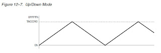 There are three modes to operate Timer_A. Which one we use depends entirely on the application. The first mode is what we call the continuous mode: Timer_A acts just like a 16-digit, binary odometer; it counts from 0 to 0xFFFF and then "rolls over" to 0 again. The second mode is called up mode; here, just like in continuous mode, it counts up and rolls over to 0. This mode, however, lets you choose how high up the timer counts before rolling over. The third mode, up/down mode, is similar to up mode in that you can program the upper limit. It differs in that rather than rolling over to 0, it turns around and counts down to 0. When you would choose to use the different modes may or may not be immediately obvious, so as you peruse articles on this and other sites, take note of how each mode is used when you see them in examples.
Registers
First, note that there is also a Timer_B system available in some devices, which in most respects is just like Timer_A. None of the value line devices have this system, so if you're eager to use this peripheral in another device, learn about Timer_A and then refer to the Family User's Guide for more information.
A timer is really nothing more than a counting mechanism that is tied to some type of regular interval provided by a clock. The Timer_A peripheral is what we call a 16-bit timer. This definition simply means that the timer counts from 0 in binary to 0b1111111111111111, or 0xFFFF in hex, 65,535 in decimal. Simple enough, and very useful when we know how to manipulate the behavior of the timer.
Timer Modes
Timer Modes


In addition to the three ways of counting in Timer_A, there are also a few ways we can make use of the counter. Timer_A has the ability to set "checkpoints" in its counting (Value Line devices only have two, but other devices have a third). TI calls these checkpoints Capture/Compare Registers. The most basic use of these registers is to set values at which the counter flags the processor to do something special. In fact, one of these registers is what is used to set the upper limit in up and up/down mode. The other register only flags the processor and allows the timer to keep on counting. (This is also the behavior of the first register in continuous mode.)
This type of use is the Compare mode of the register; we set a value that is compared to the current count in Timer_A. If the values are equal, it signals that's the case to the processor. Capture mode behaves a little differently; the timer waits for some type of signal (often from some sort of input) and then records the current value of the timer in the register without stopping the timer, somewhat like the lap time function of a stopwatch.
Registers
With so many ways to use Timer_A, you can probably imagine it corresponds to a lot of registers in the MSP430 to use and control the timer. There are, in fact, at least seven registers used in any device with the Timer_A peripheral. Let's take a look at each of these in more detail. In your Family User's Guide, turn to pages 12-20 through 12-23 to see the register maps.
- TACTL -- The Timer_A Control Register is used to set up the link between the timer and a clock and select the mode used.
- The TASSELx bits (8 and 9) tell the timer which clock to use as its source.
- The clock frequency can be divided by a further factor of 2, 4, or 8 using the IDx bits (6 and 7). (Note that this is further division to any divisions done from the clock source for the clock itself; you could potentially have a total division of up to 64 from your clock source for this peripheral.)
- The MCx bits (4 and 5) select the particular mode for the timer to use. Note particularly that setting these bits to 0 (the default setting on POR) halts the timer completely.
- TACLR is bit 2. If you write a 1 to this bit, it resets the timer. The MSP430 will automatically reset this bit to zero after resetting the timer.
- TAIE and TAIFG (bits 0 and 1) control the ability of the timer to trigger interrupts; more on this soon!
- TAR -- The Timer_A Register is the actual counter; reading this register reports the current value of the counter.
- TACCRx -- The Timer_A Capture/Compare Registers, of which there are two in the value line devices (TACCR0 and TACCR1) are where particular values we want to use are stored. In compare mode, we write values here where we want the timer to signal an event. Particularly, TACCR0 is used to store the value to which we want Timer_A to count in up and up/down mode. In capture mode, the processor will record the value of TAR when the MSP430 is signaled to do so.
- TACCTLx -- The Timer_A Capture/Compare Control Registers correspond to the TACCRx registers. These set the behavior of how the CCR's are used.
- CMx (bits 14 and 15) change what type(s) of signals tell the timer to perform a capture.
- CCISx (bits 12 and 13) select where the input signals are taken.
- SCS and SCCI (bits 11 and 10 respectively) change the synchronicity; the timer normally operates asynchronously to the input signals. (Yeah, I don't entirely understand this yet either. Watch for a future post to explain this further.)
- CAP (bit 8) changes whether capture mode (1) or compare mode (0) is used.
- OUTMODx (bits 5-7) select various output modes for the CCR's signal when the timer flags a capture or compare event.
- CCIE and CCIFG (bits 4 and 0) are more interrupts associated with the CCR's.
- CCI and OUT (bits 3 and 2) are the input and output for the CCR.
- COV (bit 1) is the capture overflow; this bit is set to 1 if two captures are signaled before the first capture value is able to be read.
- TAIV -- The Timer_A Interrupt Vector Register; since there are multiple types of interrupts that can be flagged by Timer_A, this register holds details on what interrupts have been flagged.
- The only bits used here are bits 1-3 (TAIVx), which show the type of interrupt that has happened, allowing us to take different actions to resolve the different types of interrupts.
There's an awful lot of information to cover to fully explain these registers, unfortunately, so we'll look at some examples of how to use the Timer_A as a means to illustrate what many of these bits do and how to use them. Before getting to that, though, we'll need to take a look at these interrupts, and that will be the topic of the next post. Hopefully we've been able to learn a little about the overall function of the Timer_A peripheral. Shortly we'll be able to put it to use in our MSP430 designs.
30 July 2010
Design Note: Using Outputs to Control Loads
In my plant-watering project, I need to control a relay switch to turn a water pump on and off. I chose this nice, inexpensive relay to do the job, and confirmed that 3V does indeed close the switch in the relay. If I connect the coil to the output of the MSP430 and set a high value on the pin, however, nothing happens.
The reason is that the MSP430 GPIO pins are limited in the amount of current they can source/sink. According to the G2x11 datasheet, the total output for P1 should not exceed +/- 48 mA. (This is also true for any of the Value Line devices.) Omron's datasheet for the G5LE shows that the power consumption of its coil is 400 mW, which means at 3.6 V provided by the LaunchPad, it draws 111 mA, well above what the MSP430 can do!
 Fortunately, there's an easy way around this that requires just a few inexpensive components. A fellow ham, N1HFX, has an excellent write up on transistor switches that includes an example for a relay switch. I've borrowed his schematic image and changed the values to what I've used for my relay. Some external parts won't need the diode, but it's cheap insurance for any inductive circuits like a mechanical relay. I'm using the same power source as for the chip (from the USB port via the LaunchPad for testing, but eventually a couple of AA batteries), but it's also possible to use a different supply, and even (with some careful design) use a different voltage. Just be certain that your current draw from the MSP430 does not exceed its limits.
One thing to keep in mind with this circuit is that rather than the switch being on with logic high, it's on with logic low. Since I want the switch off by default, I need to be sure that I've initialized the output pin to a high value before setting it as an output.
(Thanks N1HFX, de KE7BFA!)
The reason is that the MSP430 GPIO pins are limited in the amount of current they can source/sink. According to the G2x11 datasheet, the total output for P1 should not exceed +/- 48 mA. (This is also true for any of the Value Line devices.) Omron's datasheet for the G5LE shows that the power consumption of its coil is 400 mW, which means at 3.6 V provided by the LaunchPad, it draws 111 mA, well above what the MSP430 can do!
One thing to keep in mind with this circuit is that rather than the switch being on with logic high, it's on with logic low. Since I want the switch off by default, I need to be sure that I've initialized the output pin to a high value before setting it as an output.
(Thanks N1HFX, de KE7BFA!)
29 July 2010
Tutorial 08-b: Configuring the DCO
The MSP430's Digitally Controlled Oscillator is one of the most important peripherals to be able to manage. It's the easiest of the clock sources to configure, as it requires no external parts and is controlled completely by software. The DCO (within the BCS+) is configured with two registers: DCOCTL and BCSCTL1. Look up the maps of these two registers in the x2xx Family User's Guide, page 5-14.
 This image comes directly from the User's Guide, and explains how to select the different possible frequencies for the DCO. The total range of frequencies is divided into 16 overlapping ranges. So Range 7's low end overlaps Range 6's high end, and Range 7's high end overlaps Range 8's low end. Make sense? Ok, each range is further subdivided into 8 possible frequencies. If you plot all of these out, you get something similar to the above image, but with 16 lines instead of the three representative lines shown here. There are then 128 distinct frequencies available to the DCO, with some overlap of course.
Registers
We are able to select the frequency we use with the RSELx bits in BCSCTL1 (select range 0 to 15) and the DCOx bits in DCOCTL (select step 0 to 7). How do we know which pair we want? The device-specific datasheet should give you some help in that regard. For the G2x11, we see the DCO frequency table on page 26. For any device, this table will either list the typical value for a sample of selections, or a set of min/max values for the selection set. (Note: As of this writing, the current revision of the G2x11 datasheet (SLAS695B) is printed incorrectly, giving typical values for some selections and min/max values for others. In future revisions of the document it will likely be changed to only one or the other.) TI uses an ordered pair notation to describe the DCO setting, such as (8,2) for Range 8, Step 2 (or DCO 2 to use their term). We'll use that notation from now on to describe DCO settings with the convention DCO(r, s) where r is the range value and s is the step value.
As an example, note that DCO(6,3) is typically 0.80 MHz (or 800 kHz), while DCO(13,3) is 7.8 MHz. Note that the table only lists DCO(r,3) pairs for each range, and also values for DCO(0,0) and DCO(15,7), the low and high end of the DCO values. What about all the others? At the bottom of the table, there are two values called SRSEL and SDCO. These values give the ratio of subsequent ranges and steps as SRSEL = (r+1,s)/(r,s) and SDCO = (r,s+1)/r(s), allowing you to get a value for any of the possible combinations. For example, DCO(6,4) would be SDCO * DCO(6,3), or in the case of the G2211, 1.08*0.80 Mhz = 0.864 MHz. DCO(6,7) would be SDCO * DCO(6,6) = SDCO * (SDCO * DCO(6,5)) and so on, so a general formula would be DCO(r,s+n) = SDCO^n * DCO(r,s). (Note that you can get the lower step values with negative n, eg. DCO(6,1) = DCO(6,3-2) = SDCO ^ (-2) * DCO(6,3).)
One final topic before getting to the code; each MSP430 device comes with at least one calibrated value for the DCO. These values are found for each individual chip at the fabrication facility and programed into the information memory section of the flash memory. The values are not necessarily the same for my G2211 as it is for yours, but if you ever accidentally (or intentionally) erase the calibration values, TI does provide a program that will recalibrate the DCO and write the values to the memory for later use. (You should be able to find this program in the code examples you can download for your device. The G2xx code can be obtained here, and the program is called msp430x20xx_dco_flashcal.c.) The G2x11 devices only have one calibrated frequency at 1 MHz.
Example
Now for the practical part. Fire up CCS with your launchpad, and enter the debugging mode with any program you have. We're not going to actually run the program, just look at some of the registers as they come up by default. The MSP430 x2xx devices supposedly default to a 1.1 MHz DCO. What value actually comes up? In the debugger, open up a view of the registers, and find the BCS+ registers under System_Clock. For the G2211, the registers start with values of 0x60 for DCOCTL and 0x87 for BCSCTL1. Expand the registers to look at the individual bits, and we can see that RSEL is 0b0111, or 7, and DCO is 0b011, or 3. The default setting for the DCO is DCO(7,3), which according to the datasheet is between 0.80 MHz and 1.50 MHz. The actual value depends on your unit, the temperature, pressure, phase of the moon... ok, not really the moon phase, but you get the idea. If you happen to have an oscilloscope, we can actually look at the frequency by using the alternate function for P1.4-- the SMCLK can be driven by the DCO and put on this pin for external use.
Let's write up some code to actually change the DCO now. We're mostly interested in manipulating the DCOx and RSELx bits, which are bits 5-7 in DCOCTL and 0-3 in BCSCTL1 respectively. When we've selected the pair of values we want, we can change those bits in code. For example, if we want to change to DCO(12,2), we want 0b1100 for RSELx and 0b010 for DCOx. We can set these values in our code with the following:
BCSCTL1 &= ~(BIT0 + BIT1); // set bits 0 and 1 to 0
DCOCTL |= BIT6; // set bit 6 to 1
Does the order matter? Well, keep in mind the frequency will change with every step. So after the first line, assuming we have the default configuration found above, the bits have changed to 0b0100, putting us in DCO(4,3). The second line moves us to DCO(12,3). The third line moves us to DCO(12,2), making the last step redundant. If we had started by setting bits 2 and 3 in RSELx, we would have stepped from DCO(7,3) to DCO(15,3), putting a really high frequency on everything. That may not be an issue, but if you have any sensitive components you might consider stepping rather than jumping up to higher frequencies. If MCLK is driven by DCO (it is by default) you may find some problems as the higher frequencies may be above the 16 MHz limit for the processor. Going the other direction, jumping down puts the DCO at a really low frequency, which slows down the operation of the subsequent steps, but shouldn't cause any serious trouble.
Setting to calibrated values is much easier, since CCS provides us with shortcuts to those values:
BCSCTL1 = CALBC1_1MHZ;
DCOCTL = CALDCO_1MHZ;
Those two lines are all that's needed to set the DCO at exactly 1 MHz! (Within 3%, anyway.)
I've written some code in dcodemo_g2211.c that gives an example of how to use the DCO in a program. Browse through it and try running it on your launchpad to see how it works. The program simply flashes the LED with a delay loop and waits for the user to press the button. The program then changes the DCO frequency, and re-flashes the LED. Since the frequency increases, however, the LED flash is much faster, even though it uses the same delay loop! The DCO is controlling the operating speed of the processor, and so the for loop steps through much more quickly. Another button press slows down the DCO and re-flashes the LED, this time at a slow rate. Another button press returns the LaunchPad to the original state, and the program runs through again.
We haven't covered all the features of the DCO yet, and will discuss them as we progress further. Next we'll talk about the use of timers in the MSP430. As always, feel free to discuss and ask questions about what you've read here!
Reader Exercise: My G2211 unit that came with my LaunchPad uses DCO(6,5) for the calibrated 1 MHz frequency on the DCO, and sets the MODx bits to 0b00101 (which is also 5). What does yours use? Write a program that uses the calibrated value and use the debugger to find out what the register settings are for the 1 MHz calibration on your unit. Supposedly, these are set individually to the chip, so I'd be interested to hear if anyone actually has a different value than mine!

Registers
We are able to select the frequency we use with the RSELx bits in BCSCTL1 (select range 0 to 15) and the DCOx bits in DCOCTL (select step 0 to 7). How do we know which pair we want? The device-specific datasheet should give you some help in that regard. For the G2x11, we see the DCO frequency table on page 26. For any device, this table will either list the typical value for a sample of selections, or a set of min/max values for the selection set. (Note: As of this writing, the current revision of the G2x11 datasheet (SLAS695B) is printed incorrectly, giving typical values for some selections and min/max values for others. In future revisions of the document it will likely be changed to only one or the other.) TI uses an ordered pair notation to describe the DCO setting, such as (8,2) for Range 8, Step 2 (or DCO 2 to use their term). We'll use that notation from now on to describe DCO settings with the convention DCO(r, s) where r is the range value and s is the step value.
As an example, note that DCO(6,3) is typically 0.80 MHz (or 800 kHz), while DCO(13,3) is 7.8 MHz. Note that the table only lists DCO(r,3) pairs for each range, and also values for DCO(0,0) and DCO(15,7), the low and high end of the DCO values. What about all the others? At the bottom of the table, there are two values called SRSEL and SDCO. These values give the ratio of subsequent ranges and steps as SRSEL = (r+1,s)/(r,s) and SDCO = (r,s+1)/r(s), allowing you to get a value for any of the possible combinations. For example, DCO(6,4) would be SDCO * DCO(6,3), or in the case of the G2211, 1.08*0.80 Mhz = 0.864 MHz. DCO(6,7) would be SDCO * DCO(6,6) = SDCO * (SDCO * DCO(6,5)) and so on, so a general formula would be DCO(r,s+n) = SDCO^n * DCO(r,s). (Note that you can get the lower step values with negative n, eg. DCO(6,1) = DCO(6,3-2) = SDCO ^ (-2) * DCO(6,3).)
One final topic before getting to the code; each MSP430 device comes with at least one calibrated value for the DCO. These values are found for each individual chip at the fabrication facility and programed into the information memory section of the flash memory. The values are not necessarily the same for my G2211 as it is for yours, but if you ever accidentally (or intentionally) erase the calibration values, TI does provide a program that will recalibrate the DCO and write the values to the memory for later use. (You should be able to find this program in the code examples you can download for your device. The G2xx code can be obtained here, and the program is called msp430x20xx_dco_flashcal.c.) The G2x11 devices only have one calibrated frequency at 1 MHz.
Example
Now for the practical part. Fire up CCS with your launchpad, and enter the debugging mode with any program you have. We're not going to actually run the program, just look at some of the registers as they come up by default. The MSP430 x2xx devices supposedly default to a 1.1 MHz DCO. What value actually comes up? In the debugger, open up a view of the registers, and find the BCS+ registers under System_Clock. For the G2211, the registers start with values of 0x60 for DCOCTL and 0x87 for BCSCTL1. Expand the registers to look at the individual bits, and we can see that RSEL is 0b0111, or 7, and DCO is 0b011, or 3. The default setting for the DCO is DCO(7,3), which according to the datasheet is between 0.80 MHz and 1.50 MHz. The actual value depends on your unit, the temperature, pressure, phase of the moon... ok, not really the moon phase, but you get the idea. If you happen to have an oscilloscope, we can actually look at the frequency by using the alternate function for P1.4-- the SMCLK can be driven by the DCO and put on this pin for external use.
Let's write up some code to actually change the DCO now. We're mostly interested in manipulating the DCOx and RSELx bits, which are bits 5-7 in DCOCTL and 0-3 in BCSCTL1 respectively. When we've selected the pair of values we want, we can change those bits in code. For example, if we want to change to DCO(12,2), we want 0b1100 for RSELx and 0b010 for DCOx. We can set these values in our code with the following:
BCSCTL1 &= ~(BIT0 + BIT1); // set bits 0 and 1 to 0
BCSCTL1 |= BIT2 + BIT3; // set bits 2 and 3 to 1
DCOCTL &= ~(BIT5 + BIT7); // set bits 5 and 7 to 0DCOCTL |= BIT6; // set bit 6 to 1
Does the order matter? Well, keep in mind the frequency will change with every step. So after the first line, assuming we have the default configuration found above, the bits have changed to 0b0100, putting us in DCO(4,3). The second line moves us to DCO(12,3). The third line moves us to DCO(12,2), making the last step redundant. If we had started by setting bits 2 and 3 in RSELx, we would have stepped from DCO(7,3) to DCO(15,3), putting a really high frequency on everything. That may not be an issue, but if you have any sensitive components you might consider stepping rather than jumping up to higher frequencies. If MCLK is driven by DCO (it is by default) you may find some problems as the higher frequencies may be above the 16 MHz limit for the processor. Going the other direction, jumping down puts the DCO at a really low frequency, which slows down the operation of the subsequent steps, but shouldn't cause any serious trouble.
Setting to calibrated values is much easier, since CCS provides us with shortcuts to those values:
BCSCTL1 = CALBC1_1MHZ;
DCOCTL = CALDCO_1MHZ;
Those two lines are all that's needed to set the DCO at exactly 1 MHz! (Within 3%, anyway.)
I've written some code in dcodemo_g2211.c that gives an example of how to use the DCO in a program. Browse through it and try running it on your launchpad to see how it works. The program simply flashes the LED with a delay loop and waits for the user to press the button. The program then changes the DCO frequency, and re-flashes the LED. Since the frequency increases, however, the LED flash is much faster, even though it uses the same delay loop! The DCO is controlling the operating speed of the processor, and so the for loop steps through much more quickly. Another button press slows down the DCO and re-flashes the LED, this time at a slow rate. Another button press returns the LaunchPad to the original state, and the program runs through again.
We haven't covered all the features of the DCO yet, and will discuss them as we progress further. Next we'll talk about the use of timers in the MSP430. As always, feel free to discuss and ask questions about what you've read here!
Reader Exercise: My G2211 unit that came with my LaunchPad uses DCO(6,5) for the calibrated 1 MHz frequency on the DCO, and sets the MODx bits to 0b00101 (which is also 5). What does yours use? Write a program that uses the calibrated value and use the debugger to find out what the register settings are for the 1 MHz calibration on your unit. Supposedly, these are set individually to the chip, so I'd be interested to hear if anyone actually has a different value than mine!
Subscribe to:
Posts (Atom)